众所周知,精密仪器构件的表面形貌对其性能影响重大,当下,纳米级精度的3D表面轮廓测量在工业制造业等众多领域存在广泛需求。近日,剑桥南京中心CEO及学术主任,中心 “应用于3D表面分析的全息干涉仪”项目(下简称“全息干涉仪”项目)首席研究员初大平教授接受了中心采访,他从高精度3D表面测量的行业瓶颈出发,系统阐释了在研项目的解决方案、技术和工程优势及发展前景。
在科学研究和应用转化一线活跃将近四十年的初教授,拥有十分广泛的研究背景。物理学科出身的他,博士毕业后先后从事非挥发性铁电、薄膜晶体管、生物传感器等半导体器件,液晶、有机发光等显示器件,喷墨打印、增材制造、互补晶体管3D 打印构造等印刷电子方面的应用研究,科研履历完整,覆盖从材料到器件再到产品化的全过程。
近十年来,初教授将科研兴趣汇聚在光全息研究以及相关领域。光全息研究范围广泛,他的研究不仅涵盖光源本身、空间光调制器,还利用光全息研究重新构造头戴式/车载/裸眼3D等相关显示系统。此外,他的研究领域还涉足全光网领域,研发波长复用等全光网中最为关键的光开关器件,凭借核心技术,由他指导的相关衍生公司已成功被收购,顺利完成商业化步入下一阶段的产品开发。
现初大平教授任职剑桥大学终身讲席教授、先进光电子中心主任以及光子器件与传感器中心主任,本次专访围绕的中心项目“应用于3D表面分析的全息干涉仪”,就隶属于初教授近年来所专注的光全息和空间光调制器研究领域,项目致力于实现高精度的3D表面测量。
谈及项目科研初衷,初教授表示,伴随加工精度提高,以半导体材料为代表的精密器件构造的精度要求,已经从常规测量下的毫米级,到机械测量下的微米级,如今已至纳米量级,“相应地,探求相对便捷、高效、低成本的精密表面测量手段也愈加迫切”。
初教授介绍到,当前纳米级精度的表面形貌测量方法,主要分为接触式与非接触式两类,他对现有主流方法的优劣与短板均进行系统剖析。
接触式手段以探针式表面高度测量、原子力显微镜的纳米级/亚纳米级精度测量为主,该方法虽在常规条件下即可操作,但也有明显缺陷:一方面,探针的接触,无法避免地会对样品表面产生影响和损害;另一方面,纳米级精度使用的探针极细,单次测量范围狭小,进而探针在样品表面机械扫描的面积受限,通过逐行扫描拼接出二维的3D高度图,操作费时,扫描速度及与表面的关系会产生一系列人为误差,故而探针法对较大面积大视角的高精度测量存在瓶颈。
非接触式手段中,扫描电镜虽然可以运用电子束观察到样品的表面形貌,但无法测出样品表面起伏的确切数值,难以直接进行定量测量;
传统光学干涉测量仪,运用相干光束在表面反射获得干涉条纹,根据光程差换算相位差,也可测算出样品表面的纳米级形貌变化,但初教授指出,该非接触式方法同样存在如下弊端:
所运用的聚焦光束单次只能测量表面一个狭小的光点,视场有限,同探针法和扫描电镜一样,不便于进行大面积表面测量,制约采样速度,限制对大样品表面的快速测量,而且测量高度上限通常只能达到几百微米;
光程差信息由两部分组成,一部分反映样品表面高低起伏的形貌,另一部分反映光学镜头等光学系统构件的不平整度所带来的相差,后者属于干扰信息,如何在高精度下将两部分予以区别,并对后者进行校正和消除,亦是光学干涉仪面临的重大技术挑战。
核心聚焦:实现大视场、
大高差、异质材料的3D表面分析
如何实现精度更高、测量更快、视场更大的非接触式3D表面分析?针对上述传统光学干涉测量仪的痛点,由初教授所主持的“全息干涉仪”项目给出了解决思路。

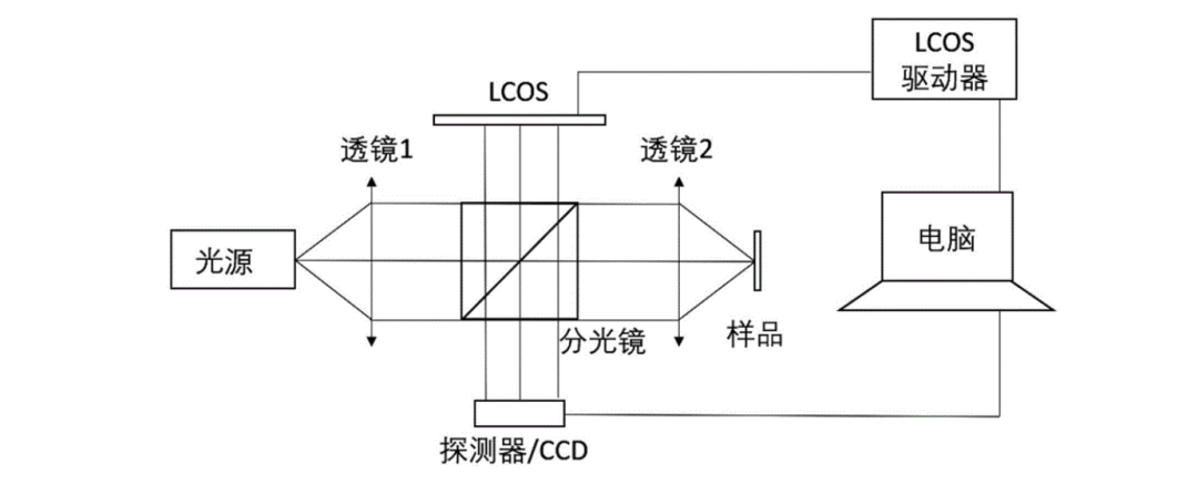
“该项目在传统光学干涉仪中引入了全息法和纯相位LCOS(硅基液晶)空间光调制器,来综合解决低效和低精度的难题”,初大平教授解释到,其一,使用全息法,能同时产生成千上万万个光点,可运用光束扫描实现厘米、分米乃至更大视场下的多点并行测量,采样速度较之单点扫描的方式大为提升;其二, LCOS空间光调制器高度可调,可逐点校正系统相差,实现空间光调制器相差部分的精确标定,所测量的干涉条纹信息,可补偿中间的光学器件硬件不平整带来的相差,缩小测量误差,这是通常的测量手段难以实现的。
“能够解决干涉条纹周期性带来的误差,精准地测量异质材料样品表面,是该项目的两大技术贡献”,初教授进一步阐释到,“这两个一直以来是干涉仪测量的棘手难题”。
就干涉条纹的周期性问题而言,相位干涉中最关键的要素是相位差,光程差改变一个波长,带来的相位差是2π,如果测量物体表面高度差超过一个波长,鉴于干涉条纹的周期性,会导致干涉条纹重复出现。换句话说,面对纵向测量范围超过波长量级的大高差表面形貌,除了要将样品表面与不平整光学构件带来的相差区别开来,还要将重复的干涉条纹和产生它的光程差一一对应,实现整体干涉条纹的无缝拼接与推演。项目率先引入空间光调制器,有望突破大高差的高精度表面分析束缚。
就样品表面材料的异质问题而言,同质材料的样品具备同一反射率,反射强度和相位延迟保持一致,意味着相位差主要源于表面的高差变量,故高精度测量难度相对较低;但测量异质材料的表面时,不同部分使用不同材料、不同材料拥有不同反射率,相位差既来自表面高差,也来自表面材料的差异(如半导体器件的表面会同时使用半导体、介电质、金属等数种材料,又如细胞表面的异质构造),制约测量精度。目前主流测量方法对此不予区分,较少考虑材料对相位差的影响。项目率先利用空间光调制器,可探索异质样品表面的高精度测量。
基于可实现大视角的、大高差的、异质材料的高精度3D表面测量的技术优势,“全息干涉仪”项目应用前景相当广阔。从宏观尺度下,实现如大型天文望远镜光学镜头在数米范围下的高精度测量;到中观尺度下,应用于如精密车床转动轴、发动机部件、调节仪器等精密仪器的加工;再到微观尺度下,实现如集成电路、MEMS设备、微纳器件超材料结构高度的刻蚀、生物医学细胞检测等,该项目都存在应用空间。
同时,该项目的工程制造优势也相当显著。项目采用不同于以往干涉仪的核心器件装置,而将LCOS设备集成到干涉仪中,采用全息法以数字化方式将干涉条纹的信息融合到全息图中,用数字光学的方式来代替传统固定化的模拟光学,大大缓解了传统干涉仪产业对高精度光学镜头、昂贵压电驱动器件的依赖,降低了仪器重量和成本。“鉴于核心器件的差异,意味着全息干涉仪项目需要搭建不同于传统干涉仪的上下游产业链条,这可与现有的干涉仪产业形成互补效应”,初教授进一步表示。
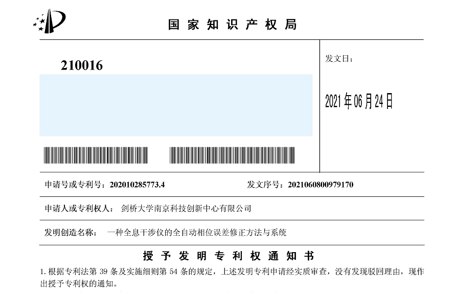
从上游的技术研发而言,初教授团队突破LCOS器件以往多用于投影光强显示的局限,在剑桥大学,团队拥有涵盖空间光调制器开发、超净组装、操作以及全息图高速生成全流程的完整实验设备线,积累多年丰富经验,已开发出整套的相位调节技术,实现了两π相位间6/8/10 Bit的相差测量,团队的LCOS产品组装工艺处于世界领先水平,并已成立创新公司为行业头部企业提供相关服务;在南京,该项目Co-PI剑桥大学博士后邓远博和本地合作专家东南大学教授杨海宁在光学测量架构方面均拥有成熟的工程化经验,并且引入了多位全职科研人员,目前已获批一项“一种全息干涉仪的全自动相位误差修正方法与系统”技术发明专利。
 从下游的技术成果转化而言,高度匹配的产业集群相当重要。在国内工业4.0迅猛发展的背景下,“应用于3D表面分析的全息干涉仪”项目落地南京江北新区,与江北新区聚焦打造“芯片之城”、“基因之城”的愿景不谋而合。初教授表示,新区不仅集聚了包括台积电等在内的大量优秀半导体企业,还形成了包括生物医药谷等在内健康医疗产业集群,这为项目在区域内开展精密器件加工和细胞级别生物检测等潜在合作创造契机,为产业化的协同创新提供机遇。
“科研要以应用为导向,要把技术用起来”,初教授最后强调到,“技术用起来最好标志是产品化、有市场,能够让用户受益于新技术”。聚焦项目的产业化执行路径,他表示,项目计划以开发第一代工程样机为抓手,开发出“标准全息干涉仪”为产业化的初始范本,将形成的平台化技术进行验证演示,启动创新公司或进行技术转让,以一至两项细分需求为突破口,围绕具体应用领域开发相应的检测仪器、延伸出不同系列的测量产品,不断根据市场需求进行产品的迭代优化,从而为不同的场景提供极致的测量效果。
Interview with PIs of the CUNJC
Professor Daping Chu:
Better 3D surface measurement technology, "
large field of view, large height difference, heterogeneous materials, high precision"
As we all know, the surface morphology of precision instrument components has a significant impact on its performance. At present, 3D surface profile measurement with nanometer precision is widely required in many fields such as industrial manufacturing. Recently, Professor Daping Chu, the CEO and academic director of the Centre, PI of the Centre’s project "Holographic Interferometer for 3D Surface"(hereinafter referred to as the project), accepted an interview with the Centre. Starting from the bottleneck of high-precision 3D surface measurement, he systematically explained solutions, technical and engineering advantages, and development prospects of the project.As we all know, the surface morphology of precision instrument components has a significant impact on its performance. At present, 3D surface profile measurement with nanometer precision is widely required in many fields such as industrial manufacturing. Recently, Professor Daping Chu, the CEO and academic director of the Centre, PI of the Centre’s project "Holographic Interferometer for 3D Surface"(hereinafter referred to as the project), accepted an interview with the Centre. Starting from the bottleneck of high-precision 3D surface measurement, he systematically explained solutions, technical and engineering advantages, and development prospects of the project.
Professor Chu has been engaged in scientific research and achievement transformation for nearly 40 years, and has a diversified research background. With an academic background in physics, he has worked in applied research on non-volatile ferroelectrics, thin-film transistors, biosensors, liquid crystal, organic light-emitting, inkjet printing, additive manufacturing, 3D printing of complementary transistor, etc. His scientific research experience has covered the entire process from materials to devices to commercialization.
In the past ten years, Professor Chu has concentrated his scientific research interests on optical holography research and related fields. The research scope of optical holography is wide. His research not only covers the light source itself and the spatial light modulator, but also uses the research of optical holography to reconstruct related display systems such as head-mounted/vehicle/naked-eye 3D. In addition, his research field is also involved in the field of all-optical neTWorks, developing wavelength multiplexing and other most critical optical switching devices in all-optical networks. Relying on core technology, related spin-offs under his guidance have been successfully acquired, and the commercialization step has been successfully completed.
Professor Chu is currently a tenured professor at the University of Cambridge, the director of the Advanced Optoelectronics Center and the director of the Photonic Devices and Sensors Center. Focusing on his research field of optical holography and spatial light modulator, the project is committed to achieving high-precision 3D surface measurement.
Bottlenecks of 3D surface analysis
with nanometer precision
Talking about the original intention of the project, Professor Chu said that with the improvement of processing accuracy, the precision requirements of the precise instrument represented by semiconductor materials have gone from millimeter level under conventional measurement to micron level under mechanical measurement, and now it has reached nanometer level. “Correspondingly, it is increasingly urgent to search for convenient, efficient, and low-cost precision surface measurement methods."
Professor Chu introduced that the current nanometer-level precision surface measurement methods are mainly divided into two types: contact and non-contact. He systematically analyzes the advantages and disadvantages of the existing mainstream methods.
Professor Chu introduced that the current nanometer-level precision surface measurement methods are mainly divided into two types: contact and non-contact. He systematically analyzes the advantages and disadvantages of the existing mainstream methods.
The contact method is mainly based on the probe-type surface height measurement and the nanometer/sub-nanometer precision measurement of the atomic force microscope. Although this method can be operated under normal conditions, it has obvious shortcomings: on the one hand, the probe will inevitably affect and damage the sample surface; on the other hand, the probe used for nanometer precision is extremely thin, and the single measurement range is narrow, therefore the mechanical scanning area of the probe on the sample surface is limited. Splicing a two-dimensional 3D height map by scanning line by line is time-consuming, and the relationship between scanning speed and surface can cause human errors. Therefore, the probe method has bottlenecks for high-precision measurement of large areas and large viewing angles.
As for the non-contact method, although the scanning electron microscope can use the electron beam to observe the surface morphology of the sample, it cannot measure the exact value of the surface fluctuation of the sample, and it is difficult to directly perform quantitative measurement;
Traditional optical interferometers use coherent beams to reflect on the surface to obtain interference fringes. According to the optical path difference to convert the phase difference, it can also measure the nano-level morphology change of the sample surface. However, Professor Chu pointed out that the non-contact method also has the following disadvantages:
The focused beam can only measure a small spot on the surface at a time, and the field of view is limited. Like the probe method and scanning electron microscope, the sampling speed for the large sample surface is limited and the upper limit of the measurement height is usually only a few hundred microns;
The optical path difference information consists of two parts, one part reflects the undulating topography of the sample surface, and the other part reflects the phase difference caused by the unevenness of the optical lens and other optical system components. The latter belongs to interference information. How to distinguish the two parts with high precision and correct and eliminate the latter is also a major technical challenge faced by optical interferometers.
Focus: Realize 3D surface analysis
of large fieldof view, large height
difference, and heterogeneous materials
How to achieve non-contact 3D surface analysis with higher accuracy, faster measurement, and larger field of view? Aiming at the pain points of the above-mentioned traditional optical interferometers, the project led by Professor Chu gives a solution.
 "This project introduces the holographic method and pure phase LCOS (liquid crystal on silicon) spatial light modulator into the traditional optical interferometer to comprehensively solve the problem of low efficiency and low precision", Professor Chu explained. First, the holographic method can generate tens of thousands of light points at the same time, and beam scanning can be used to realize multi-point parallel measurement in centimeters, decimeters, and even larger fields of view, thus the sampling speed is greatly improved than that of single-point scanning; second, the height of the LCOS spatial light modulator is adjustable, and the system phase difference can be corrected point by point to achieve precise calibration of the phase difference part of the spatial light modulator. The measured interference fringe information can compensate for the phase difference caused by the unevenness of the optical device hardware in the middle, and reduce the measurement error, which is difficult to achieve with the common measurement methods.
"The ability to solve the error caused by the periodicity of interference fringes and accurately measure the surface of heterogeneous material samples is the two major technical contributions of this project", Professor Chu further explained, "These two have always been thorny problems in interferometer measurement. "
As far as the periodicity of interference fringes is concerned, the most critical element in phase interference is phase difference. When the optical path difference changes by one wavelength, the phase difference is 2π. If the height difference of the measured object surface exceeds one wavelength, it will cause the interference fringe to appear repeatedly due to the periodicity of the interference fringe. In other words, in the face of a large elevation difference surface morphology with a longitudinal measurement range exceeding the wavelength order, in addition to distinguishing the phase difference caused by the sample surface and the uneven optical components, we also need to correspond the repeated interference fringes to the optical path difference that produced it, so as to realize the seamless splicing and deduction of the overall interference fringes. The project is the first to introduce spatial light modulator, which is expected to break through the constraints of high-precision surface analysis with large height differences.
In terms of the heterogeneity of the surface material of samples, the sample of the same material has the same reflectivity, and the reflection intensity and phase delay remain the same, which means that the phase difference is mainly derived from the height difference variable of the surface, so the difficulty of high-precision measurement is relatively low; But when measuring the surface of a heterogeneous material, since different parts use different materials and different materials have different reflectivity, the phase difference comes from both the surface height difference and surface materials (For example, the surface of semiconductor devices may use several materials such as semiconductors, dielectrics, and metals at the same time. Another example is the heterogeneous structure of the cell surface), which restricts measurement accuracy. The current mainstream measurement methods do not distinguish this, and seldom consider the influence of the material on the phase difference. The project is the first to use spatial light modulators to explore high-precision measurement of the surface of heterogeneous samples.
Strengthening industrialization: project
application prospects and industrial chain
Based on the technical advantages that can achieve high-precision 3D surface measurement of large viewing angles, large height differences, and heterogeneous materials, the application prospect of the project is quite broad. At the macro-scale, it can help achieve high-precision measurements such as the optical lens of large astronomical telescopes in the range of several meters; at the meso-scale, it can be applied to the processing of precision instruments such as precision lathe rotation shafts, engine parts, and adjustment instruments; at the microscopic scale, there is room for application of this project to achieve high-level etching of metamaterial structures such as integrated circuits, MEMS equipment, etching of metamaterial structure of micro-nano devices, and biomedical cell detection.
At the same time, the engineering and manufacturing advantages of the project are also quite significant. The project adopts a core device that is different from the previous interferometer, and integrates the LCOS equipment into the interferometer, using the holographic method to digitally combine the interference fringe information with the hologram, and digital optics to replace the traditional immobilized analog optics, which greatly eases the traditional interferometer industry's dependence on high-precision optical lenses and expensive piezoelectric driving devices, and reduces the weight and cost of the instrument." The difference in core components means that the project needs to build an upstream and downstream industrial chain that is different from the traditional interferometer, which can form a complementary effect with the existing interferometer industry," Professor Chu further explained.
 In terms of upstream technology research and development, the team of Professor Chu broke through the limitations of LCOS devices used for projection light intensity display in the past. At the University of Cambridge, the team has a complete experimental line covering spatial light modulator development, ultra-clean assembly, operation, and high-speed hologram generation, and has developed a complete set of phase adjustment technology which achieved 6/8/10 bit phase difference measurement between 2π phases. The team’s LCOS product assembly technology is at the world’s leading level, and an innovative company has been established to provide related services to industry leaders; in Nanjing, both Dr. Deng Yuanbo, Co-PI of the project and postdOCToral fellow of Cambridge University, and local cooperative expert Professor Yang Haining from Southeast University, have rich engineering experience in optical measurement architecture. Currently, the technical invention patent "a fully automatic phase error correction method and system for holographic interferometers" applied by the Centre for the project has been approved.
In terms of the transformation of downstream technological achievements, highly matched industrial clusters are very important. In the context of the rapid development of domestic Industry 4.0, the project’s landing in Nanjing Jiangbei New Area coincides with the New Area's vision of focusing on building a "City of Chips" and "City of Genes". Professor Chu said that the New Area not only gathers a large number of excellent semiconductor companies including TSMC, but also forms a health and medical industry cluster including the Biomedicine Valley, which creates opportunities for the project to carry out potential cooperation in the region such as precision device processing and cell-level biological detection, and provides opportunities for industrialized collaborative innovation.
"Scientific research should be application-oriented, and technology should be used." Professor Chu finally emphasized that "the best sign of using technology is productization, marketability, and enabling users to benefit from new technologies." Focusing on the industrialization path of the project, he said that the project plans to develop the first-generation engineering prototype as the starting point, develop the "standard holographic interferometer" as the initial model for industrialization, and demonstrate the platform technology that has been formed to start innovative companies or carry out technology transfers. With one or two segmented requirements as a breakthrough, it will develop corresponding testing instruments around specific application areas, extend different series of measurement products, and continuously optimize products according to market needs, so as to provide the ultimate measurement effect for different scenarios.
剑桥南京中心推出「科研项目PI专访」栏目,以项目首席研究员的专业视角,立体化解读中心在研项目的学术价值、应用场景、国际合作、最新动态等,融合全球产业态势和国内产业动向,以飨同好。
The "Interview with PIs of the Centre" launched by the CUNJC comprehensively interprets the academic value, application scenarios, international cooperation, and latest developments of the center's research projects from the professional perspective of the PIs, integrating global and domestic industrial trends.


 从下游的技术成果转化而言,高度匹配的产业集群相当重要。在国内工业4.0迅猛发展的背景下,“应用于3D表面分析的全息干涉仪”项目落地南京江北新区,与江北新区聚焦打造“芯片之城”、“基因之城”的愿景不谋而合。初教授表示,新区不仅集聚了包括台积电等在内的大量优秀半导体企业,还形成了包括生物医药谷等在内健康医疗产业集群,这为项目在区域内开展精密器件加工和细胞级别生物检测等潜在合作创造契机,为产业化的协同创新提供机遇。